
Semiconductors and India: What Chips Are, the Global Value Chain, India Semiconductor Mission, New Fabs and Packaging Units, Challenges and the Way Ahead (UPSC Notes + PYQs)
UPSC has already asked about this. Read the story with these questions in mind.
What a semiconductor is
Conductors such as copper let electricity flow freely; insulators such as glass block it. A semiconductor sits in between, and adding tiny amounts of other elements, called doping, lets engineers control exactly how it conducts. Silicon is the most used; gallium arsenide, gallium nitride and silicon carbide serve special uses such as power electronics, electric vehicles and 5G. A chip, or integrated circuit, packs billions of microscopic switches called transistors onto a sliver of silicon. Smaller transistors mean faster, more efficient chips; leading-edge chips are now made at “3 nanometre” and “2 nanometre” process nodes, names that describe a generation of technology rather than a real dimension.
The value chain
| Stage | What happens | Who leads |
|---|---|---|
| Design | Engineers design the chip with software tools (EDA) | US firms (Nvidia, Qualcomm, AMD, Apple); many design centres in India |
| Equipment and materials | Lithography machines, gases, wafers | Netherlands (ASML), US, Japan |
| Fabrication (fab) | Patterns etched on silicon wafers in ultra-clean factories | Taiwan (TSMC), South Korea (Samsung), US (Intel), China |
| Assembly, testing, marking and packaging (ATMP/OSAT) | Wafers cut, chips packaged and tested | Taiwan, China, Malaysia, Vietnam |
India is strong in design, with about a fifth of the world’s chip design engineers, but until recently had no commercial fab or large packaging unit. Its only fab, the Semi-Conductor Laboratory at Mohali, makes older-node chips mainly for strategic uses.
- 1Design with EDA tools
- 2Silicon wafer prepared
- 3Patterns etched in a fab
- 4Wafers cut into dies
- 5Packaged and tested (ATMP/OSAT)
Why chips are geopolitical
Taiwan’s TSMC makes most of the world’s most advanced chips, so any conflict across the Taiwan Strait would cripple the global economy. The chip shortage of 2020-22, when car factories stood idle, showed how fragile supply chains are. The United States passed the CHIPS and Science Act (2022) with about USD 52 billion in support and imposed export controls on advanced chips and tools to China; the EU, Japan and South Korea launched their own subsidies. Countries now want “trusted” supply chains, and India pitches itself as one through partnerships such as the US-India TRUST initiative, the Quad’s semiconductor supply chain work, and agreements with Japan and Singapore.
India Semiconductor Mission
The Union Cabinet approved a ₹76,000 crore programme in December 2021, run by the India Semiconductor Mission (ISM) under MeitY. It offers fiscal support of up to 50% of project cost, on a pari-passu basis, for fabs, display fabs, compound semiconductor units and ATMP/OSAT units, with States adding their own incentives. A Design Linked Incentive scheme supports chip design start-ups, and the Chips to Startup programme trains engineers. A second phase of the mission has been announced to cover equipment, materials and more advanced nodes.
Projects approved
| Project | Type | Location |
|---|---|---|
| Micron Technology | ATMP | Sanand, Gujarat |
| Tata Electronics with PSMC (Taiwan) | Fab (28 nm and above) | Dholera, Gujarat |
| Tata Semiconductor Assembly and Test | OSAT | Jagiroad, Assam |
| CG Power with Renesas and Stars Microelectronics | OSAT | Sanand, Gujarat |
| Kaynes Semicon | OSAT | Sanand, Gujarat |
| HCL-Foxconn joint venture | Display driver chips (OSAT) | Jewar, Uttar Pradesh |
| SiCSem | Silicon carbide compound semiconductors | Odisha |
The first chips from Indian pilot lines were shown at Semicon India in 2025. Prelims 2026 tested the location of these plants.
Challenges
- Capital and time: a modern fab costs billions of dollars and takes years to build and yield well.
- Utilities: fabs need uninterrupted power and huge volumes of ultra-pure water.
- Ecosystem: specialty gases, chemicals, wafers and equipment are mostly imported.
- Skills: India has designers but few fab process engineers; ISM aims to train 85,000 engineers.
- Technology: leading nodes are controlled by a handful of firms that guard their know-how.
- Demand: plants need assured buyers; India’s electronics manufacturing is still assembly-heavy.
- Billions of dollars per fab
- Pure water and steady power
- Imported gases, chemicals and tools
- Few trained process engineers
- Closely held technology
Why it is worth it
Chips are to the digital age what steel was to the industrial age. India’s electronics demand is rising fast with phones, cars, data centres and defence systems, and a domestic base reduces the risk of supply shocks and import dependence. Packaging units create many jobs and build skills, which can then support more advanced fabs. Mature-node chips (28 nm and above), which India is targeting first, are used in cars, appliances and power systems, a large and steady market.
Way forward
Build from packaging and mature nodes upward, attract equipment and chemical suppliers into clusters at Dholera and Sanand, secure water and power, expand university courses in microelectronics, use the Design Linked Incentive to create Indian chip product companies, and deepen partnerships with the US, Japan, Taiwan and the EU for technology and markets.
Display fabs and compound semiconductors
Chips are not the only target. Screens for phones, TVs and laptops come from display fabs, almost all in China, South Korea, Japan and Taiwan, and ISM offers the same 50% support for them. Compound semiconductors such as silicon carbide and gallium nitride handle high power and frequency far better than silicon, so they are used in electric vehicle inverters, fast chargers, solar inverters, radar and 5G base stations. Because this field is newer and less crowded, India sees a chance to catch up faster here, which is why the SiCSem unit in Odisha and research at institutes such as IISc Bengaluru matter.
PYQ trend
Mains GS-III 2025 asked about the challenges of making India a semiconductor hub. Prelims 2026 asked about plant locations; older papers asked about materials such as graphene.
Semiconductors: UPSC angle
For UPSC CSE
Mains GS-III: industrial policy, technology, supply chains. Prelims: plants, materials, schemes.
Semiconductors UPSC PYQs (Prelims)
Questions UPSC has actually asked, from the official papers. Pick an option to check yourself.
Which one of the following pairs of semiconductor plants in India and their locations is not correctly matched ?
The HCL-Foxconn unit was approved in 2025 near Jewar in Uttar Pradesh (Yamuna Expressway area), not Madhya Pradesh. CG Power’s plant is at Sanand, Gujarat; Tata’s assembly and test unit is at Jagiroad, Assam; SiCSem’s silicon carbide fab is in Odisha. Answer as per the official UPSC key · Battle IAS PYQ bankAnswer (c) & why
Graphene is frequently in news recently. What is its importance?
– 1. It is a two-dimensional material and has good electrical conductivity.
– 2. It is one of the thinnest but strongest materials tested so far.
– 3. It is entirely made of silicon and has high optical transparency.
– 4. It can be used as ‘conducting electrodes’ required for touch screens, LCDs and organic LEDs.
Which of the statements given above are correct?
Graphene is a single sheet of carbon atoms in a honeycomb: two-dimensional, an excellent conductor, one atom thick yet stronger than steel, and almost transparent. That makes it good for transparent electrodes in touch screens and OLEDs. It is made of carbon, not silicon. Answer as per the official UPSC key · Battle IAS PYQ bankAnswer (c) & why
Mains PYQs on this topic
Questions from the official UPSC Mains papers (2023-2026 in the Battle IAS Mains bank), newest first. Each links to a model answer.
- UPSC Mains 2025 · GS Paper III · Q16 · 15 marks
India aims to become a semiconductor manufacturing hub. What are the challenges faced by the semiconductor industry in India ? Mention the salient features of the India Semiconductor Mission.
Quick quiz
Which stage of the chip value chain is India strongest in?
India has a large share of the world’s chip design engineers.Answer (c)
India’s first commercial semiconductor fab is being built at
Tata Electronics with PSMC at Dholera, Gujarat.Answer (b)
OSAT in semiconductors stands for
It covers packaging and testing.Answer (a)
FAQs
What is the India Semiconductor Mission?
A ₹76,000 crore programme approved in 2021, run under MeitY, that funds fabs, display fabs and packaging units with up to 50% of project cost.
What is the difference between a fab and an OSAT?
A fab makes chips on silicon wafers; an OSAT or ATMP unit cuts, packages and tests them.
Why is Taiwan so important in chips?
Its firm TSMC makes most of the world’s most advanced chips.
Which semiconductor unit is in Uttar Pradesh?
The HCL-Foxconn joint venture near Jewar, making display driver chips.
Why does India start with mature nodes?
They are cheaper to build, have steady demand in cars and appliances, and build skills for later advanced nodes.
Spotted an error? Tell us. We correct within 48 hours.
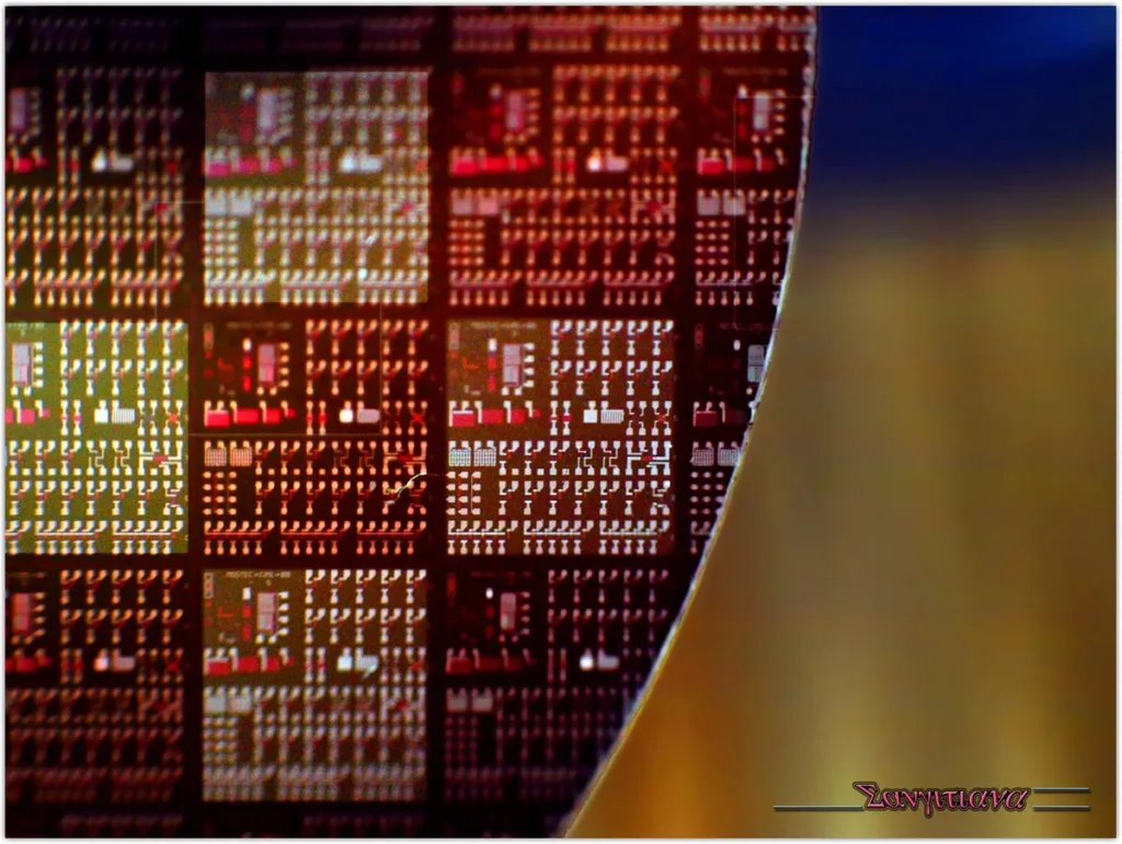
Image: Sangitiana Fararano, Wikimedia Commons, CC BY-SA 2.0
How to use this in Mains
If asked: UPSC Mains 2025, GS-III: India aims to become a semiconductor manufacturing hub. What are the challenges faced by the semiconductor industry in India ? Mention the salient features of the India Semiconductor Mission.
Quote: “Ecosystem: specialty gases, chemicals, wafers and equipment are mostly imported.”
Use it: A precise point for the 'challenges' part; add ISM incentives after it.
In the news
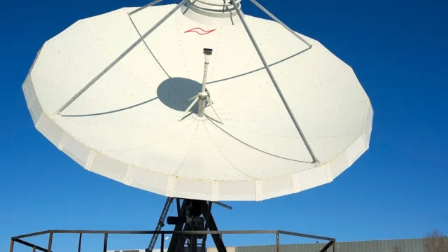
Government says satellite communication licensing is fair; three NGSO-based GMPCS licensees at same stage
On 8 October 2026 the Department of Telecommunications rejected a social media claim that satellite internet licensing is discriminatory. Three licences for Global Mobile Personal Communication by Satellite services using non-geostationary satellites have been issued; all three are going through security assessment, after which each can seek spectrum.
8 Oct 2026
National Supercomputing Mission: 40 supercomputers, 68 petaflops
A PIB backgrounder says the National Supercomputing Mission, launched in April 2015, had deployed 40 supercomputers with a combined 68 petaflops by September 2026, including 13 above 1 petaflop. The target is 50 systems above 123 petaflops. India now makes its own Rudra servers, interconnects, cooling and system software.
4 Oct 2026
India’s first 5.56 km free-space quantum key distribution link demonstrated
QNu Labs, with BISAG-N and IIT Gandhinagar, demonstrated India's first free-space quantum key distribution (QKD) link over 5.56 km on the night of 27-28 September 2026. The quantum bit error rate stayed below 5 per cent and secure keys were made at 230-260 bps, then used with BISAG-N's Vedic Kavach post-quantum cryptography platform.
3 Oct 2026
TRAI launches Digital Connectivity Rating platform for buildings
On 25 September 2026 TRAI launched the Digital Connectivity Rating (DCR) Platform and a mobile app. Property managers apply for a rating, registered rating agencies test the building, and anyone can search rated properties and verify the certificate by QR code before buying or renting.
25 Sep 2026